Component Burn In: Why Your Electronics Manufacturing Depends On ItAuthor : Adrian September 01,dek solder paste printer 2025Table of ContentsIn the fast-paced world of electronics manufacturing, ensuring the reliability and longevity of your products is non-negotiable. One critical process that stands between you and potential product failures is electronic component burn-in testing. But what exactly is burn-in testing, and why is it so vital? Simply put, burn-in testing stresses electronic components under extreme conditions to identify early failures before they reach the market. This process is a cornerstone of quality control, helping manufacturers deliver dependable products and avoid costly recalls or customer dissatisfaction. In this detailed guide, we’ll explore the importance of burn-in testing, dive into various component reliability testing methods, and explain how burn-in testing for component failurecan save your production line from disaster. Whether you’re an engineer, a quality assurance specialist, or a business owner in the electronics industry, understanding this process can make a significant difference in your manufacturing success.
What Is Electronic Component Burn-In Testing?Burn-in testing is a quality assurance method used to detect early failures in electronic components by subjecting them to accelerated stress conditions. These conditions often include elevated temperatures, high voltages, and extended operation times that mimic years of real-world use in just a few hours or days. The goal is to “weed out” defective parts that might fail prematurely, ensuring that only reliable components make it into the final product. Think of burn-in testing as a rigorous boot camp for your electronics. Just as soldiers are tested under tough conditions to ensure they’re ready for battle, components are pushed to their limits to confirm they can handle the demands of everyday use. For example, a semiconductor might be tested at 125°C with a voltage of 5.5V (slightly above its rated 5V) for 48 hours to simulate stress over a 5-year lifespan. This process helps identify weak components that could fail due to manufacturing defects, material flaws, or design issues.
Why Burn-In Testing Is Crucial for Electronics ManufacturingThe electronics industry thrives on trust. Customers expect devices—whether smartphones, medical equipment, or automotive systems—to work flawlessly from day one. A single failure can damage a brand’s reputation and lead to financial losses. This is where burn-in testing plays a pivotal role. Let’s break down why it’s indispensable:
For instance, in the automotive sector, a failing sensor in a vehicle’s braking system could have catastrophic consequences. Burn-in testing ensures such critical components can withstand harsh conditions like temperature swings from -40°C to 85°C and constant vibration over years of use.
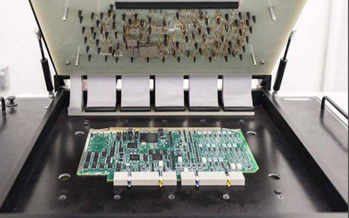
Common Component Reliability Testing MethodsBurn-in testing isn’t a one-size-fits-all process. Different components and applications require tailored approaches to ensure reliability. Below are some widely used component reliability testing methodsthat often incorporate burn-in techniques: 1. Static Burn-In TestingIn static burn-in testing, components are subjected to elevated temperatures and voltages without active operation. For example, a capacitor might be held at 105°C and 120% of its rated voltage for 24 hours. This method is effective for identifying issues like dielectric breakdown or material degradation in passive components. 2. Dynamic Burn-In TestingDynamic testing goes a step further by operating the component under stress conditions. A microcontroller, for instance, might run at full load with a clock speed of 100 MHz (its maximum rated speed) while exposed to 85°C for 72 hours. This simulates real-world usage and uncovers failures related to thermal stress or electrical overstress. 3. Temperature CyclingWhile not strictly burn-in, temperature cycling is often combined with it to test a component’s resilience to thermal expansion and contraction. A power transistor might be cycled between -55°C and 125°C over 100 cycles to ensure it can handle rapid temperature changes without cracking or delaminating. 4. High-Temperature Operating Life (HTOL)HTOL is a burn-in method specifically for active components like ICs and transistors. It involves operating the component at high temperatures (e.g., 125°C) and slightly elevated voltages for extended periods, such as 1000 hours, to predict long-term reliability. This method is common in industries where failure is not an option, such as aerospace.
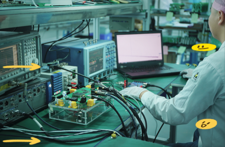
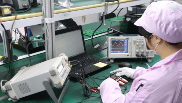
How Burn-In Testing Prevents Component FailureThe primary goal of burn-in testing for component failureis to eliminate weak links in the production chain. Electronic components can fail for various reasons—manufacturing defects, poor material quality, or design flaws. Burn-in testing accelerates the aging process to expose these vulnerabilities before they cause problems in the field. For example, a batch of resistors might have micro-cracks in their ceramic coating due to a production error. Under normal conditions, these cracks might not cause failure for months or years. However, during burn-in testing at 100°C for 48 hours, the thermal stress could widen the cracks, causing the resistor to fail. By catching this early, manufacturers can scrap or rework the defective batch, preventing costly failures in finished products. Moreover, burn-in testing provides valuable data for improving designs and processes. If a specific type of capacitor consistently fails under high-voltage burn-in conditions, engineers can investigate whether the issue lies in the material, design, or manufacturing process, leading to better products in future iterations.
Key Benefits of Burn-In Testing in Electronics ManufacturingImplementing burn-in testing offers several tangible benefits that directly impact the bottom line and customer satisfaction. Let’s explore these advantages in detail:
Challenges in Implementing Burn-In TestingWhile burn-in testing is undeniably beneficial, it’s not without challenges. Manufacturers must balance the advantages with practical considerations to make the process cost-effective and efficient.
Despite these challenges, advancements in testing technology are making burn-in more accessible. Automated testing systems can now handle large batches of components simultaneously, reducing time and cost while maintaining accuracy.
Best Practices for Effective Burn-In TestingTo maximize the benefits of electronic component burn-in testing, manufacturers should follow these best practices:
Future Trends in Burn-In TestingAs electronics become more complex and compact, burn-in testing methods are evolving to keep pace. Here are some emerging trends shaping the future of component reliability testing methods:
These innovations promise to make burn-in testing faster, cheaper, and more accurate, ensuring that even the most advanced electronics meet reliability standards.
Conclusion: Invest in Burn-In Testing for Long-Term SuccessIn the competitive world of electronics manufacturing, cutting corners on quality control is a recipe for disaster. Electronic component burn-in testingis not just a checkbox—it’s a strategic investment in your product’s reliability and your brand’s reputation. By identifying early failures, improving component lifespan, and reducing field issues, burn-in testing helps you deliver products that stand the test of time. Whether you’re producing consumer gadgets, industrial equipment, or life-saving medical devices, integrating robust burn-in testing for component failureinto your workflow is essential. With the right methods, equipment, and expertise, you can ensure that every component in your assembly meets the highest standards of performance and durability. At ALLPCB, we understand the importance of reliability in every stage of electronics production. Our commitment to quality ensures that your projects benefit from cutting-edge testing and manufacturing processes. Ready to elevate your product reliability? Partner with us to build electronics that last. Share · · · · The Role of Flux in PCB Wave Soldering: Selection, Application, and Residue RemovalMarch 16, 2026PCB wave soldering flux types include rosin, water-soluble, and no-clean options with varying activity levels for oxide removal and solder flow. This guide covers selection criteria, spray foam drop-jet application methods, residue removal processes, and alternatives like nitrogen blanketing to boost joint reliability and yields for engineers. Article Achieving Uniform Solder Fillets in PCB Wave Soldering: Process ControlMarch 16, 2026Achieve uniform solder fillets in PCB wave soldering with process control strategies. Optimize flux, preheat, wave height, conveyor speed for consistent fillet shape, height, and wetting balance. Includes visual inspection tips and troubleshooting for reliable through-hole assemblies. Boost quality in production. Article Optimizing Conveyor Speed for Efficient PCB Wave SolderingMarch 16, 2026Learn PCB wave soldering conveyor speed calculation to manage dwell time, immersion depth, and throughput effectively. Electric engineers get practical steps, best practices, and troubleshooting tips for higher process efficiency and fewer defects in wave soldering operations. Article Understanding IPC Standards for PCB Surface Finishes: Ensuring Quality and ComplianceMarch 11, 2026Understand IPC standards IPC 4552 ENIG and IPC 4553 immersion silver for PCB surface finishes. Ensure compliance, enhance solderability, and prevent common defects to achieve reliable, high quality circuit boards. Article Miniaturization Challenges in PCB AssemblyMarch 11, 2026Navigate the complexities of high density interconnect PCB assembly and precise component placement. Learn to tackle miniaturization challenges, from tiny part handling to thermal stress, ensuring robust and reliable electronics. Article High Speed Routing Techniques: PCBMarch 11, 2026Master high speed routing in PCBs to ensure signal integrity and minimize electromagnetic interference. Learn essential techniques for robust designs, from controlled impedance to differential pair strategies. Prevent performance issues and achieve reliable electronics. ArticleGet Instant PCB |